Large-Scale Monolithic Fabrication of III–V Vertical Nanowires on a Standard Si(100) Microelectronic Substrate
Résumé
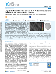
Vertical III−V nanowires are of great interest for a large number of applications, but their integration still suffers from manufacturing difficulties of these one-dimensional nanostructures on the standard Si(100) microelectronic platform at a large scale. Here, a top-down approach based on the structure of a thin III−V epitaxial layer on Si was proposed to obtain monolithic GaAs or GaSb nanowires as well as GaAs−Si nanowires with an axial heterostructure. Based on a few complementary metal−oxide− semiconductor-compatible fabrication steps, III−V nanowires with a high crystalline quality as well as a uniform diameter (30 nm), morphology, positioning, and orientation were fabricated. In addition, the patterning control of nanowires at the nanoscale was thoroughly characterized by structural and chemical analyses to finely tune the key process parameters. To properly control the morphology of the nanowires during reactive-ion etching (RIE), the balance between the plasma properties and the formation of a protective layer on the nanowire sidewall was studied in detail. Furthermore, high-resolution microscopy analyses were performed to gain a better understanding of the protective layer's composition and to observe the crystalline quality of the nanowires. This approach paves the way for the possible scale-up integration of III−V-based nanowire devices with conventional Si/complementary metal−oxide−semiconductor technology.
Domaines
Sciences de l'ingénieur [physics]
Fichier principal
 22_Lecestre acsomegaLarge-Scale Monolithic Fabrication of III−V Vertical Nanowires on a Standard Si100 Microelectronic Substrate.pdf (6.17 Mo)
Télécharger le fichier
| Origine | Fichiers éditeurs autorisés sur une archive ouverte |
|---|